

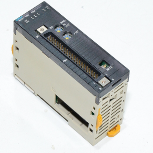
OMRON C500-CT012 PLC
OMRON C500-CT012 PLC
9-16 Extended Data Memory (EM) Area
The EM Area is supported by the CJ1 and CJ1-H CPU Units only. It is divided
into 7 banks (0 to C) that each contain 32.768 words. EM Area addresses
range from E0_00000 to EC_32767. This data area is used for general data
storage and manipulation and is accessible only by word.
Data in the EM Area is retained when the PLC’s power is cycled or the PLC’s
operating mode is changed from PROGRAM mode to RUN/MONITOR mode
or vice-versa.
Although bits in the EM Area cannot be accessed directly, the status of these
bits can be accessed with the BIT TEST instructions, TST(350) and
TSTN(351).
Bits in the EM Area cannot be force-set or force-reset.
Specifying EM Addresses
1.2.3…
There are two ways to specify an EM address: the bank and address can be
specified at the same time or an address in the current bank can be specified
(after changing the current bank, if necessary). In general, we recommend
specifying the bank and address simultaneously.
1. Bank and Address Specification
With this method, the bank number is specified just before the EM address.
For example, E2_00010 specifies EM address 00010 in bank 2.
2. Current Bank Address Specification
With this method, just the EM address is specified. For example, E00010
specifies EM address 00010 in the current bank. (The current bank must
be changed with EMBC(281) to access data in another bank. A301 con
tains the current EM bank number.)
The current bank will be reset to 0 when the operating mode is changed
from PROGRAM mode to RUN/MONITOR mode, unless the IOM Hold Bit
(A50012) is ON. The current bank is not changed as the program proceeds
through cyclic tasks and the current bank will be returned to its original val
ue (in the source cyclic task) if it has been changed in an interrupt task
Words in the EM Area can be indirectly addressed in two ways: binary-mode
and BCD-mode.
Binary-mode Addressing (@E)
When a “@” character is input before a EM address, the content of that EM
word is treated as binary and the instruction will operate on the EM word in
the same bank at that binary address. All of the words in the same EM bank
(E00000 to E32767) can be indirectly addressed with hexadecimal values
0000 to 7FFF and words in the next EM bank (E00000 to E32767) can be
addressed with hexadecimal values 8000 to FFFF.
@E1_00100
@E00100
0200
0200
E1_00512
Address actually used.
E0_00512
Address actually used.
BCD-mode Addressing (
*
(When the current
bank is bank 0.)
E)
When a “*” character is input before a EM address, the content of that EM
word is treated as BCD and the instruction will operate on the EM word in the
same bank at that BCD address. Only part of the EM bank (E00000 to
E09999) can be indirectly addressed with BCD values 0000 to 9999.
*E1_00100
*E00100
0200
0200
E1_00200
Address actually used.
C500-CT012
E0_00200
Address actually used.
(When the current
bank is bank 0.)
Part of the EM Area can be converted for use as file memory with settings in
the PLC Setup. All EM banks from the specified bank (EM File Memory Start
ing Bank) to the last EM bank will be converted to file memory.
Once EM banks have been converted to file memory, they cannot be
accessed (read or written) by instructions. An Illegal Access Error will occur if
a file-memory bank is specified as an operand in an instruction.
The following example shows EM file memory when the EM File Memory
Starting Bank has been set to 3 in the PLC Setup.
Example:
EM File Memory Starting Bank
EM bank number
set to 3 in the PLC Setup
EM file memory
(Cannot be accessed
from instructions.)
9-17 Index Registers
The sixteen Index Registers (IR0 to IR15) are used for indirect addressing.
Each Index Register can hold a single PLC memory address, which is the
absolute memory address of a word in I/O memory. Use MOVR(560) to con
vert a regular data area address to its equivalent PLC memory address and
write that value to the specified Index Register. (Use MOVRW(561) to set the
PLC memory address of a timer/counter PV in an Index Register.)
Note Refer to Appendix D Memory Map of PLC Memory Addresses for more details
on PLC memory addresses