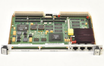
Motorola MVME5101-0131 Single Board Computer
Motorola MVME5101-0131 Single Board Computer
The MVME5100 is a high-performance VME single board computer featuring the
Motorola Computer Group (MCG) PowerPlus II architecture with a choice of PowerPC®
processors—either Motorola’s MPC7400 with AltiVec™ technology for algorithmic
intensive computations or the low-power MPC750.
As of the printing date of this manual, the MVME5100 is available in the configurations
shown below. All models of the MVME5100 are available with either VME SCANBE
front panel (-01×1) or IEEE 1101 compatible front panel (-01×3).
MVME5100-0131
MVME5100-0161
MVME5100-0133
MVME5100-0163
MVME5101-0131
MVME5101-0161
MVME5101-0133
MVME5101-0163
The MVME5100 is a state-of-the-art Single Board Computer. It
incorporates Motorola’s PowerPlus II architecture with a choice of
PowerPC processors—either Motorola’s MPC7400 with AltiVec™
technology for algorithmic intensive computations or the low-power
MPC750.
The MVME5100 incorporates a highly optimized PCI interface and
memory controller enabling up to 582MB memory read bandwidth and
640 MB burst write bandwidth.
The on-board Hawk ASIC provides the bridge function between the
processor’s bus and the PCI bus. It provides 32-bit addressing and 64-bit
data; however, 64-bit addressing (dual address cycle) is not supported. The
ASIC also supports various processor external bus frequencies up to
10MHz
Feature Specification
Microprocessors and
Bus Clock Frequency
•MPC7400 @400 MHz Internal Clock Frequency
•MPC750 @450 MHz Internal Clock Frequency
• Bus Clock Frequency up to 100 MHz
L2 Cache (Optional) • 1MB (MPC750) or 2MB (MPC7400) using burst-mode
SRAM modules.
Memory • EEPROM, on-board programmable
• 1MB via two 32-pin PLCC/CLCC sockets;
16MB Surface Mount
Main Memory
(SDRAM)
• PC100 ECC SDRAM with 100 MHz bus
• 32MB to 512MB on board, expandable to
1GB via RAM500 memory mezzanine
NVRAM • 32KB (4KB available for users)
Memory Controller • Hawk System Memory Controller (SMC)
PCI Host Bridge • Hawk PCI Host Bridge (PHB)
Interrupt Controller • Hawk Multi-Processor Interrupt Controller (MPIC)
Peripheral Support • Dual 16550-Compatible Asynchronous Serial Port’s
Routed to the Front Panel RJ45 Connnector (COM1) and
On-Board Header (COM2)
• Dual Ethernet Interfaces, one routed to the Front Panel
RJ45. one routed to the Front Panel RJ45 or optionally
routed to P2. RJ45 on MVME761
VMEbus • Tundra Universe Controller, 64-bit PCI
• Programmable Interrupter & Interrupt Handler
• Programmable DMA Controller With Link List Support
• Full System Controller Functions
PCI/PMC/Expansion • Two 32/64-bit PMC Slots with Front-Panel I/O Plus,
P2 Rear I/O (MVME2300 Routing)
• One PCI Expansion Connector (for the PMCSpan)
Miscellaneous • Combined RESET and ABORT Switch
MVME5101-0131
• Status LEDs
Form Factor • 6U VME
Memory maps
The following sections describe the memory maps for the MVME5100.
Processor Memory Map
Following a reset, the memory map presented to the processor is identical
to the CHRP memory map described in the PowerPlus II Engineering
Specification listed in Appendix A, Related Documentation.
The MVME5100 is fully capable of supporting both the PREP and the
CHRP processor memory maps with ROM/FLASH size limited to
16MBytes and RAM size limited to 1GB.
PCI / VME Memory Map
Following a reset, the Hawk ASIC disables all PCI slave map decoders. As
stated above, the MVME5100 is fully capable of supporting both the PREP
and the CHRP PCI and VME memory maps.
System Bus
The following sections describe the processor system bus for the
MVME5100.
Processors
The MVME5100 has the BGA foot print that supports the MPC7400
processor. The maximum external processor bus speed is 100 MHz. Parity
checking is supported for the system address and data busses.
Processor Type Identification
The type of the processor can be determined by reading the Processor
Version Register (PVR). The PVR value for the MPC7400 processor is
0x000C0100h
Processor PLL Configuration
The processor internal clock frequency (core frequency) is a multiple of
the system bus frequency. The processor has four configuration pins,
PLL_CFG[0:3], for hardware strapping of the processor core frequency
between 2x and 8x the system bus frequency, in 0.5x steps.
The PLL configuration shall be dynamic at power-up and be dependent
upon the existence of a memory mezzanine attached to the host board.
L2 Cache
The MVME5100 incorporates an L2 cache using a 2-way, set-associative
tag memory located in the MPC7400 processor, with external direct
mapped synchronous SRAMs for data storage. The external SRAMs are
accessed through a dedicated L2 cache port on the processor.
L2 Cache SRAM Size
The L2 cache port will support SRAM configurations of 1MB or 2MB.
The L2 cache size is defined by reading the Vital Product Data (VPD)
SROM and programming the L2SIZ bits in the processor’s Cache Control
Register (L2CR).
Cache Speed
The MPC7400 cache port provides the clock for the synchronous SRAMs.
This clock is generated by dividing the processor core frequency.
Available core-to-cache dividers range from 1 to 4. in .5 steps.
The core-to-cache ratio is selected by reading the VPD SROM and
programming the L2CLK bits of the processor’s Cache Control Register.
Flash Memory
The MVME5100 Flash memory characteristics are fully compatible with
those specified in the Hawk’s specification for Flash Blocks
A and B
System Memory
MVME5100 system memory characteristics are fully compatible with
those of the Hawk ASIC for memory Blocks A, B, C, and E.
The on-board memory Blocks are Blocks A and B. The optional add-on
mezzanine memory Blocks are C (first mezzanine attached) and
E (second mezzanine attached).
Serial Presence Detect (SPD) Definitions
The MVME5100 SPD uses the SPD JEDEC standard definition. On board
SPD for SDRAM Bank A or both A and B of the Hawk shall be accessed
at Address $A8 . Only Bank A or Banks A and B will be populated. If both
banks A and B are populated, they will be the same speed and memory
size. Memory Mezzanine 1 SPD for SDRAM Bank C of the Hawk shall be
accessed at Address $AA. Memory Mezzanine 2 SPD for SDRAM Bank
E of the Hawk shall be accessed at address $AC.
Hawk ASIC
Hawk I2C interface and configuration information
The Hawk ASIC has an I2C (Inter-Integrated Circuit) two-wire serial
interface bus: Serial Clock Line (SCL) and Serial Data Line (SDA)
composed of two 256 x 8 Serial EEPROM’s.
This interface has master-only capability and is used to communicate the
configuration information to a slave I2C serial EEPROM. A seperate
EEPROM is used to maintain the configuration information related to the
board (Vital Product Data, User configuration Data, etc.) and a seperate
EEPROM is used for on-board Memory Subsystem Data (MSD).
If a optional memory mezzanine is used, that mezzanine shall contain a
seperate EEPROM with its own memory subsystem data. Each slave
device connected to the I2C bus is software addressable by a unique
address.
There can be seven slave devices connected to the I2C bus on the
MVME5100. The Vital Product Data (VPD) address shall be $A0. The
User configuration Data (UPD) address shall be $A2.
The on-board MSD address (Memory Bank A and B) shall be $A8. The
optional Memory Mezzanine 1 MSD addresses shall be $AA (Memory
Bank C) and $AC (Memory Bank E) for mezzanine 2.
The IPMC761 VPD address shall be $A4. A digital thermometer
(DS1621) I2C address shall be $96. Some configuration options in the
Hawk ASIC must be configured at power-up reset time before software
performs any accesses to it. Other configuration information is needed by
software to properly configure the Hawk’s control registers. This
information can be obtained from devices connected to the I2C bus.