MOTOROLA MVME162-522A 01-W3960B/61C Embedded Controller
MOTOROLAMVME162-522A 01-W3960B/61C Embedded Controller
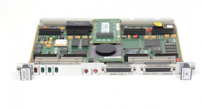
Front Panel Indicators (DS1 – DS4)
There are eight LEDs on the MVME162 front panel: FAIL, STAT, RUN, SCON,
LAN, FUSE, SCSI, and VME.
FAIL LED (red). Lights when the BRDFAIL* signal line is active. Part of
DS1.
STAT LED (yellow). Driven by the MC68040 status lines on the MVME162.
Lights when a halt condition from the processor is detected. Part of DS1.
RUN LED (green). Lights when the local bus TIP* signal line is low. This
indicates one of the local bus masters is executing a local bus cycle. Part of
DS2.
SCON LED (green). Lights when the VMEchip2 in the MVME162 is the
VMEbus system controller. Part of DS2.
LAN LED (green). Lights when the LAN chip is local bus master. Part of
DS3.
FUSE LED (green). Lights when power is available to the transceiver
interface (the MVME162 supplies +12V power to the LAN Ethernet
transceiver interface through a fuse). Part of DS3.
SCSI LED (green). Lights when the SCSI chip is local bus master. Part of
DS4.
VME LED (green). Lights when the board is using the VMEbus (VMEbus
AS* line asserted by the VMEchip2) or when the board is accessed by the
VMEbus (VMEchip2 is the local bus master). Part of DS4
Memory Maps
There are two points of view for memory maps:
The mapping of all resources as viewed by local bus masters (local bus
memory map)
MVME162-522A
The mapping of onboard resources as viewed by VMEbus masters
(VMEbus memory map)
Local Bus Memory Map
The local bus memory map is split into different address spaces by the
Transfer Type (TT) signals. The local resources respond to the normal access
and interrupt acknowledge codes.
Normal Address Range
The memory map of devices that respond to the normal address range is
shown in the following tables. The normal address range is defined by the TT
signals on the local bus. For the MVME162. transfer types 0. 1. and 2 define the
normal address range. Table 3-1 defines the entire map ($00000000 to
$FFFFFFFF). Many areas of the map are user-programmable, and suggested
uses are shown in the table. The cache inhibit function is programmable in the
MC68xx040 MMU. The onboard I/O space must be marked ‘‘cache inhibit’’
and serialized in its page table. Table 3-2 further defines the map for the local
I/O devices
The EPROM and Flash are sized by the MCchip ASIC from an
8-bit private bus to the 32-bit MPU local bus. Because the
device size is less than the allocated memory map for some
entries, the device contents repeat for those entries.
If jumper GPIO3 is installed, the Flash device is accessed. If
GPIO3 is not installed, the EPROM is accessed.
6. The Flash and EPROM are sized by the MCchip ASIC from an
8-bit private bus to the 32-bit MPU local bus. Because the
device size is less than the allocated memory map for some
entries, the device contents repeat for those entries.
If jumper GPIO3 is installed, the PROM device is accessed. If
GPIO3 is not installed, the Flash is accessed.
7. These areas are not decoded unless one of the programmable
decoders are initialized to decode this space. If they are not
decoded, an access to this address range will generate a local
bus timeout. The local bus timer must be enabled.
Table 3-2 focuses on the ‘‘Local I/O Devices’’ portion of the local bus main
memory map.
Writes to the LCSR in the VMEchip2 must be 32 bits. LCSR
writes of 8 or 16 bits terminate with a TEA signal. Writes to the
GCSR may be 8. 16 or 32 bits. Reads to the LCSR and GCSR
may be 8. 16 or 32 bits. Byte reads should be used to read the
interrupt vector.
4. This area does not return an acknowledge signal. If the local
bus timer is enabled, the access times out and is terminated by
a TEA signal.
Size is approximate.
6. Port commands to the 82596CA must be written as two 16-bit
writes: upper word first and lower word second.
7. Refer to the Flash and EPROM Interface section in the MCchip
description in Chapter 3.
Detailed I/O Memory Maps
Tables 3-3 through 3-12 provide detailed memory maps for the VMEchip2. the
MCchip, the Zilog Z85230 serial communications controller, the Intel 82596CA
LAN controller, the NCR 53C710 SCSI controller, the IPIC chip, and the
MK48T08 BBRAM/TOD Clock.
| NI | SCXI-1104C |
| NI | SCXI-1600 |
| NI | SCXI-1304 |
| NI | SCXI-1325 |
| NI | SCXI-1141 |
| NI | SCXI-1124 |
| NI | SCXI-1001 |
| NI | PXI-7340 |
| NI | GPIB-140A |
| NI | 161-0348-00 |
| NI | SCXI-1346 |
| NI | SCXI-1324 |
| NI | SCXI-1160 |
| NI | PCI-6224 |
| NI | 192061B-02 |