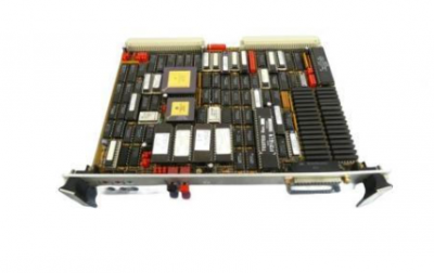
MOTOROLA MVME162-10 Embedded Controller
MOTOROLAMVME162-10 Embedded Controller
Related Documentation
The following publications are applicable to the MVME162 and may provide
additional helpful information. If not shipped with this product, they may be
purchased by contacting your local Motorola sales office. Non-Motorola
documents may be purchased from the sources listed
The following publications are available from the sources indicated.
Versatile Backplane Bus: VMEbus, ANSI/IEEE Std 1014-1987. The Institute of
Electrical and Electronics Engineers, Inc., 345 East 47th Street, New York, NY
10017 (VMEbus Specification). This is also available as Microprocessor system
bus for 1 to 4 byte data, IEC 821 BUS, Bureau Central de la Commission
Electrotechnique Internationale; 3. rue de Varembé, Geneva, Switzerland.
ANSI Small Computer System Interface-2 (SCSI-2), Draft Document X3.131-198X,
Revision 10c; Global Engineering Documents, P.O. Box 19539. Irvine, CA 92714.
IndustryPack Logic Interface Specification, Revision 1.0; GreenSpring Computers,
Inc., 1204 O’Brien Drive, Menlo Park, CA 94025.
82596CA Local Area Network Coprocessor data sheet, order number 290218; and
82596 User’s Manual, order number 296853; Intel Corporation, Literature
Sales, P.O. Box 58130. Santa Clara, CA 95052-8130.
NCR 53C710 SCSI I/O Processor Data Manual, order number NCR53C710DM;
and NCR 53C710 SCSI I/O Processor Programmer’s Guide, order number
NCR53C710PG; NCR Corporation, Microelectronics Products Division,
Colorado Springs, CO.
MVME162-10
MK48T08(B) Timekeeper™ and 8Kx8 Zeropower™ RAM data sheet in Static
RAMs Databook, Order Code DBSRAM71; SGS-THOMPSON Microelectronics
Group; North & South American Marketing Headquarters, 1000 East Bell
Road, Phoenix, AZ 85022-2699.
Z85230 Serial Communications Controller data sheet, Zilog Inc., 210 Hacienda
Ave., Campbell, CA 95008-6609.
28F008SA Flash Memory Data Sheet, Order Number 290435-001; Intel Literature
Sales, P.O. Box 7641. Mt. Prospect, IL 60056-7641.
28F020 Flash Memory Data Sheet, Order Number 290245-003; Intel Literature
Sales, P.O. Box 7641. Mt. Prospect, IL 60056-7641.
Support Information
You can obtain connector interconnect signal information, parts lists, and
schematics for the MVME162 free of charge by contacting your local Motorola
sales office
Manual Terminology
Throughout this manual, a convention is used which precedes data and
address parameters by a character identifying the numeric format as follows:
$
dollar
% percent
specifies a hexadecimal character
specifies a binary number
& ampersand specifies a decimal number
Unless otherwise specified, all address references are in hexadecimal.
An asterisk (*) following the signal name for signals which are level-significant
denotes that the signal is true or valid when the signal is low.
An asterisk (*) following the signal name for signals which are edge-significant
denotes that the actions initiated by that signal occur on high-to-low
transition.
In this manual, assertion and negation are used to specify forcing a signal to a
particular state. In particular, assertion and assert refer to a signal that is active
or true; negation and negate indicate a signal that is inactive or false. These
terms are used independently of the voltage level (high or low) that they
represent.
In this manual, MVME712 series transition module refers generically to the
MVME712-12. MVME712-13. MVME712A, MVME712AM, or MVME712M.
MVME712x transition module refers to the closely related MVME712-12.
MVME712-13. MVME712A, or MVME712AM (not to the MVME712M).
References to a specific module use the complete designation of that module.
Data and address sizes are defined as follows:
A byte is eight bits, numbered 0 through 7. with bit 0 being the least
significant.
A word is 16 bits, numbered 0 through 15. with bit 0 being the least
significant.
A longword is 32 bits, numbered 0 through 31. with bit 0 being the least
significant
Introduction
This chapter provides unpacking instructions, hardware preparation
guidelines, and installation instructions for the MVME162 Embedded
Controller. Hardware preparation for the MVME712 series transition
modules is described in separate manuals; refer to the Related Documentation
section in Chapter 1
Hardware Preparation
To produce the desired configuration and ensure proper operation of the
MVME162. you may need to carry out certain modifications before installing
the module.
The MVME162 provides software control over most options: by setting bits in
control registers after installing the MVME162 in a system, you can modify its
configuration. (The MVME162 registers are described in Chapter 4. and/or in
the MVME162 Embedded Controller Programmer’s Reference Guide as listed in
Related Documentation in Chapter 1.)
Some options, however, are not software-programmable. Such options are
controlled by manual installation or removal of header jumpers or interface
modules
Figure 2-1 illustrates the placement of the switches, jumper headers,
connectors, and LED indicators on the MVME162. Manually configurable
items include:
SIM selection for serial port B configuration (J10)
System controller selection (J1)
Synchronous clock selection (J11) for Serial Port 1/Console
Synchronous clock selection (J12) for Serial Port 2
SRAM backup power source selection (J20)
EPROM size selection (J21)
General-purpose readable register configuration (J22)
The MVME162 has been factory tested and is shipped with the configurations
described in the following sections. The MVME162’s required and factory
installed Debug Monitor, MVME162Bug (162Bug), operates with those factory
settings.
SIM Selection
Port B of the MVME162’s Z85230 serial communications controller is
configurable via a serial interface module (SIM) which is installed at connector
J10 on the MVME162 board. Four serial interface modules are available:
EIA-232-D (DCE and DTE)
EIA-530 (DCE and DTE)
You can change Port B from an EIA-232-D to an EIA-530 interface (or vice
versa) by mounting the appropriate serial interface module. Port B is routed
(via the SIM at J10) to the 25-pin DB25 front panel connector marked SERIAL
PORT 2.
For the location of SIM connector J10 on the MVME162. refer to Figure 2-1.
Figure 2-2 illustrates the secondary side (bottom) of a serial interface module,
showing the J1 connector which plugs into SIM connector J10 on the
MVME162. Figure 2-3 (sheets 3-6), Figure 2-4 (sheets 3-4), and Figure 2-5
illustrate the configurations available for Port B.
For the part numbers of the serial interface modules, refer to Table 2-1. The
part numbers are ordinarily printed on the primary side (top) of the SIMs, but
may be found on the secondary side in some versions.
If you need to replace an existing serial interface module with a SIM of another
type, go to Removal of Existing SIM below. If there is no SIM on the main board,
skip to Installation of New SIM.